Nodemcu ESP8266 Pinout, Specs, Versions with detailed board layout
NodeMCU esp8266 wifi module is an open-source, low-cost, low-power MCU(microcontroller unit) development board. It has 17 GPIO pins(11 are Digital I/O pins), out of which one pin is an analog pin, 4 pins support PWM, 2 pairs are for UART(UART0 and UART1), and supports 1x SPI and 1x I2C protocol.
NodeMCU ESP8266 has 128Kb of RAM, 4 MB of Flash memory, and a maximum clock speed of 160MHz(80 -160). The operating current is 80mA(average).
The ESP8266 Integrates an 802.11b/g/n HT40 Wi-Fi transceiver chip for WiFi connectivity and gives it the additional advantage of creating its network thus allowing other devices to connect directly to it.
Note: When ESP8266 was released, its open-source firmware was called Nodemcu by the developers. But now the term “Nodemcu” usually refers to the ESP8266 Wifi module.
Table of Contents
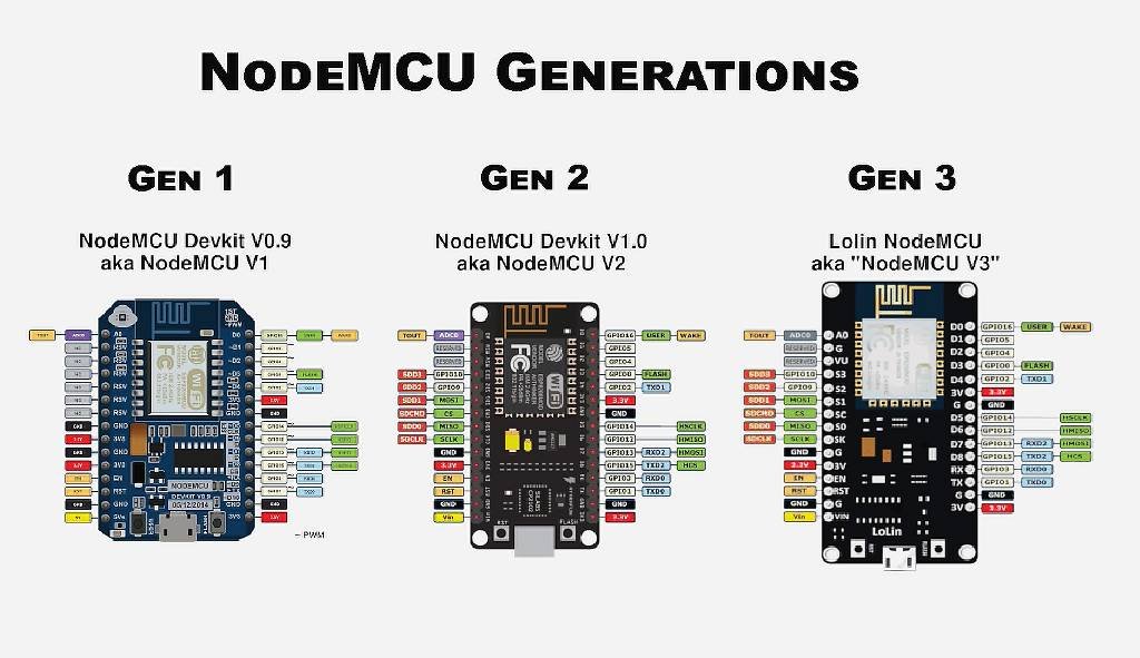
Nodemcu versions or generations:
As of now, there are three official versions of the Nodemcu: Nodemcu Devkit 0.9 or Nodemcu V1, Nodemcu Devkit 1.0 or Nodemcu V2, and Lolin Nodemcu or Nodemcu V3.
Nodemcu generations or versions
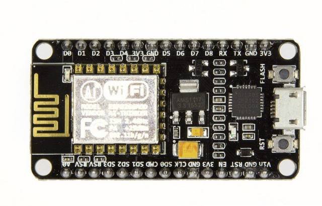
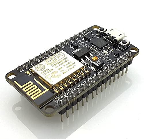
Nodemcu Esp8266 packaging style
Two main packaging types of Nodemcu are available in the market: Amica and LoLin.
Amica Nodemcu package
The Amica Nodemcu has narrow pin spacing and measures 49mm x 26mm with a standard pin space of 0.1″ between pins and 0.9″ between rows.
Nodemcu esp8266 board in Amica package
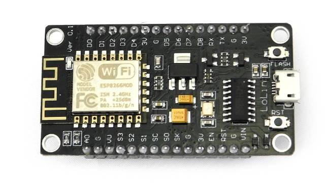
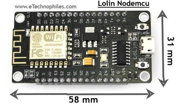
LoLin nodemcu package
The Lolin Nodemcu has a wider pin spacing and larger board layout than the Amica package. It measures 58mm x 32mm with a pin spacing of 0.1″ between pins and 1.1″ between rows.
LoLin Nodemcu ESP8266 Board
Note: The Amica NodeMCU is approximately 25% smaller in size than a closely compatible LoLin style NodeMCU.
Note: The LoLin board has 2 extra pins: VU and Ground pin. The VU pin is directly connected to the USB port power pin which can deliver 5V if the board is powered using a USB.
NodeMCU esp8266 wifi module is mostly used for IoT-based projects. By using NodeMCU ESP8266 Wifi Module, IoT applications become easier and cheaper.
Please note that the ESP8266 is a breadboard-friendly development board. And at its heart is a wifi module called ESP-12E. The ESP-12E is a tiny wifi module or the miniature version of ESP8266 that gives ESP8266 the functionality of Wireless communication. You can say, it is the brain of the ESP8266 Wifi module.
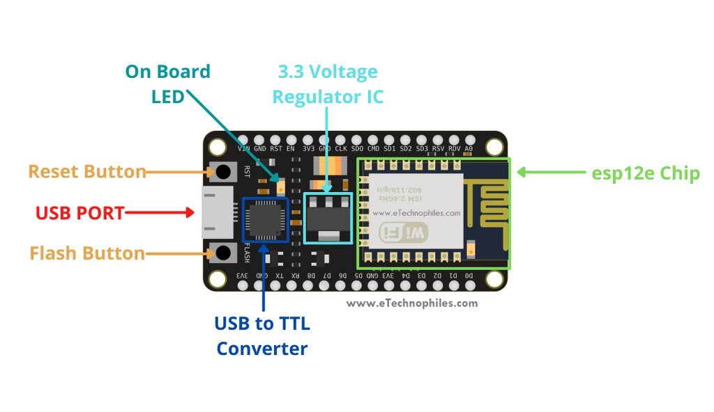
ESP8266 wifi module board layout
The Nodemcu wifi module comprises of ESP12E chip(the brain of the module), GPIO pins for easy interfacing, 3.3 Volt Voltage regulator, onboard LED, USB to serial converter IC, USB port, and more.
Nodemcu esp8266 board layout
ESP8266-12E wifi chip with antenna
This esp8266-12E or simply esp-12E chip is a member of the esp-xx series. There are 15 modules ranging from esp01 to esp15. These are mostly used for IoT applications due to their small form factor and low price.
Processor: The latest ESP12E board integrates a Tensilica LX106 32-bit RISC processor, which achieves extra-low power consumption and reaches a maximum clock speed of 160 MHz.
Uploading a program in ESP-12E using the micro USB cable is difficult as it requires a separate 3.3 voltage regulator, reset button, some resistors, and a USB to TTL converter IC.
But the development board Nodemcu ESP8266 module has everything mentioned above, thus it is easy to program it from your laptop/PC. Nodemcu ESP8266 has an Esp12e chip, a USB port to upload programs, and for power supply. It also has a reset and boot button.
Hence the Nodemcu is a better choice over the esp12e chip as it is easy to use, is breadboard-friendly, and comes at the same price.
Voltage regulator AMS1117
The esp12e chip works on 3.3 Volts. But since a micro USB cable provides 5 Volts, the Nodemcu has an on-board 3.3 V voltage regulator which is AMS1117.
USB to TTL/serial converter
To program the board using a USB cable, the USB to TTL/UART converter IC is needed. Nodemcu ESP8266 has CP2102 USB to UART bridge controller IC (in SMD QFN-28 package). Some old ESP8266 boards use CH340G USB to TTL converter IC (in SMD SOP-16 package).
Usually, the Lolin Nodemcu has CP2102 and Amica Nodemcu has CH340G USB to TTL converter IC.
Flash button
The boot or flash button is used while uploading the program. If you hold it down and press the EN/RST, the ES8266 will restart in flashing/uploading mode
Let’s have a look at the specifications of NodeMCU.
Microcontroller
ESP-8266 32-bit
NodeMCU Model
Amica(official)
Clock Speed
80-160 MHz
USB to Serial
CP2102
USB Connector
Micro USB
Operating Voltage
3.3V
Input Voltage
4.5V-10V
Flash Memory/SRAM
4 MB / 128 KB
GPIO Pins
17
Digital I/O Pins
11
Analog In Pins
1
PWM Pins
4
ADC Range
0-3.3V
UART/SPI/I2C
2 / 1 / 1
WiFi Built-In
802.11 b/g/n
Temperature Range
-40C – 125C
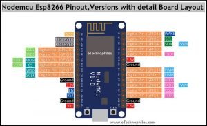
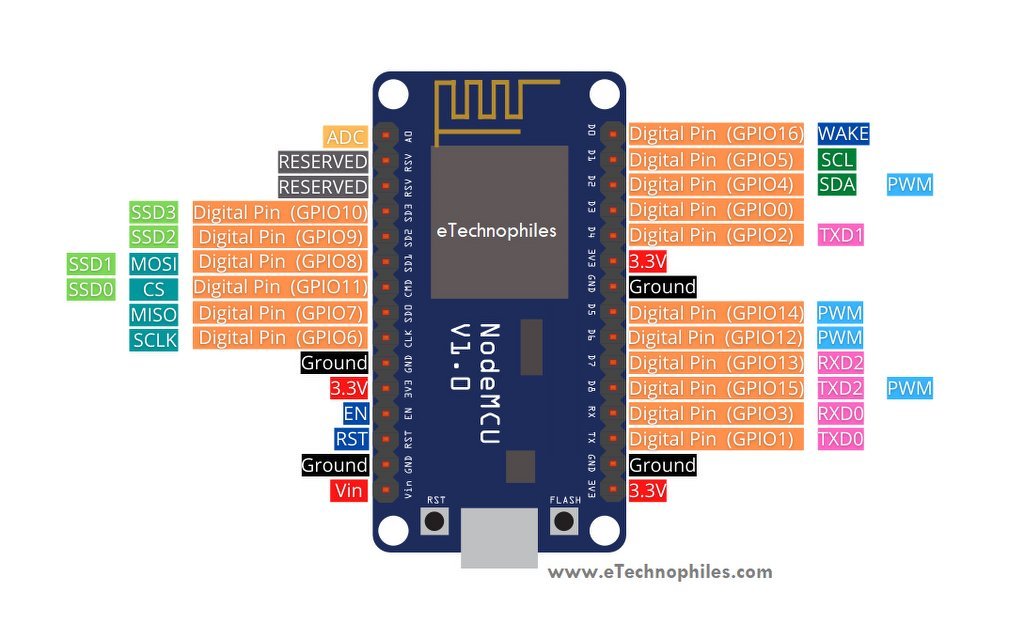
Nodemcu ESP8266 pinout
Nodemcu esp8266 pinout
As shown in the above image, there is a total of 17 GPIO(General Purpose Input Output) pins. Out of which only 11 pins are best to use. These 11 pins are mentioned in the table given below. We can use those pins as an input or output.
Pin Name
GPIO
Input
Output
D0
16
pull-up
pull-up
D1
5
OK
OK
D2
4
OK
OK
D3
0
pull-up
OK
D4
2
pull-up
OK
D5
14
OK
OK
D6
12
OK
OK
D7
13
OK
OK
D8
15
pull-down
OK
RX
3
pull-up
NO
TX
1
NO
pull-up
A0
ADC0
Analog
NO
Power pins
Vin: This pin can be used to power the esp8266 board. Up to 5V can be supplied to it. The Vin pin can be used to directly supply the Nodemcu esp8266 and its peripherals if you have a regulated 5V voltage source. This 5 volt is then converted to 3.3 volts using a voltage regulator as the esp12e chip requires 3.3V to operate.
Note: The Lolin ESP8266 module has one extra pin called VU. If the module is powered from a USB(5V), you can get 5V from the VU pin to power the external devices.
3.3 V: The board has three 3.3V pins. While the 3.3V pin is the output of a voltage regulator (CP2102), it can be used to power up the external components.
GND: There are a total of 4 such pins.
Note: All the GPIO pins of the ESP8266 are 3.3 V compatible(I/O) and are not 5V tolerant. Supplying 5 volts or more directly to any of the pins may damage the board.
ADC(Analog to digital) channel
ESP8266 has an inbuilt 10-bit ADC or analog-to-digital converter with only one ADC channel. In other words, the board has only one analog pin to read the analog voltage values from external devices like sensors and potentiometers.
This analog pin is marked as A0 on the board as given in the pinout diagram above.
The esp8266 board has 2 UART interfaces– RX0 and TX0 are UART0, RX2 and TX2 are UART1. The UART1 is used for uploading the firmware or program.
UART0 pins
U0 TXD (GPIO1)
U0 RXD (GPIO3)
UART1 pins
U1 TXD (GPIO15)
U1 RXD (GPIO13)
SPI pins
Unlike the three UART interfaces, the Esp8266 Nodemcu has only one set of SPI pins. The SPI protocol requires 4 pins: MOSI, MISO, SCLK, and CS.
GPIO 7: MISO
GPIO 8: MISO
GPIO 6: SCLK
GPIO 11: CS
I2C pins
The ESP8266 does not support any hardware I2C protocol, but it is possible to implement it in the programming part. So you may use any GPIO pins as I2C as long as you are aware of the I2C programming. Only two pins are required for I2C: SDA and SCLK.
Usually, the following GPIOs are used as I2C pins:
GPIO 4: SDA
GPIO 5: SCL
PWM pins
The board comes with 4 PWM-enabled pins. The PWM output can be used for driving digital motors and LEDs. PWM pins on the ESP8266 board are GPIO 4, GPIO 12, GPIO 14, and GPIO 15. OR digital pins D2, D5, D6, and D8.
EN or enable pin
EN stands for Enable, which enables the esp8266 chip i.e. ESP12E when pulled high. The chip works at minimum power when the EN pin is pulled low.
RST or reset Pin
This pin resets the board when pulled low. It works like the onboard reset button.
Wake pin(D0)
This pin is used to wake up the esp8266 chip from a deep sleep.
NOTE: EN, RST, and Wake pins are called the control pins of the ESP8266 board.
Nodemcu ESP8266 datasheet(ESP-12E):
To download the datasheet of this development board, click here.
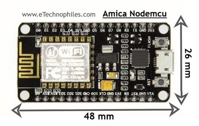
Nodemcu dimensions
Amica nodemcu V2 dimensions:
The physical dimension of Amica or Nodemcu V2 is 4.8 X 2.6 in Centimeters.
Amica Nodemcu esp8266 dimensions
LoLin nodemcu V3 dimensions:
The physical dimension of LoLin or Nodemcu V3 is 5.8 X 3.1 Centimeters.
LoLin Nodemcu ESP8266 dimensions
FAQs
Why is ESP8266 used?
ESP8266 is used for its low-cost, integrated Wi-Fi capabilities, making it ideal for IoT projects and DIY electronics. Its small form factor, low power consumption, and ease of programming contribute to its popularity in applications like home automation, sensor networks, and remote monitoring.
Is NodeMCU and Arduino same?
No, NodeMCU and Arduino are not the same. NodeMCU is a development board based on the ESP8266 microcontroller, primarily used for IoT projects and Wi-Fi connectivity. Arduino is a popular open-source electronics platform based on various microcontrollers, offering a wide range of development boards for different applications.
What language is used for NodeMCU?
NodeMCU primarily uses Lua for programming, but C/C++ (via Arduino IDE) and MicroPython are also options.
A javascript web-based Atmel AVR microcontroller fuse calculator tool. Apply chip features to see fuse bit settings or apply fuse bit settings to match against known features.
Part of programming stand-alone ATmega chips is setting the fuse bytes, these are special settings that can be used to change how the ATmega chips operate.
Some of the things you can do by changing the value of the fuses include;
select different clock sources and change how fast the chip runs,
set the minimum voltage required before the chip works.
set whether or not a boot loader is used,
set how much memory is allocated to the boot loader,
disable reset.
disable serial programming
stop eeprom data being erased when uploading a new sketch.
There are many articles online but I could not find a single source that brought all the information together and fully explain what the fuses actually do.
It is important to remember that some of the fuse bits can be used to lock certain aspects of the chip and can potentially brick it (make it unusable). However, with a bit of care it is fairly straight forward to understand and use the fuse settings.
Disclaimer, I am relatively new to programming fuses and these are notes I wrote to help me remember things. The information is based on the data sheet for the ATmega chip, internet searches, and questions I asked on forums (especially the Arduino forum).
There are 3 bytes in total:
low byte fuse,
high byte fuse,
extended fuse
There is also a forth byte that is used to program the lock bits. Lock bits are not covered by this article.
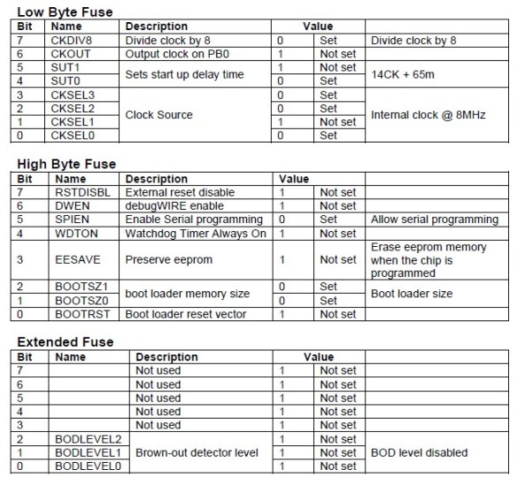
Each byte is 8 bits and each bit is a separate setting or flag. When we talk about setting/not setting, programmed/not programmed fuses we are actually using binary. 1 means not set/not programmed and a 0 (zero) means set/programmed.
When programming the fuses you can use binary notation or more commonly hexadecimal notation. For 8 bits (1 byte) we can use B11111111 or 0xFF. Both are the same value.
Note: For all fuses, a value of 1 means not set and a value of 0(zero) means set.
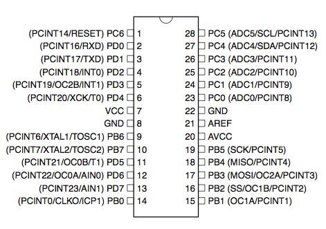
ATmega 328P 28 PDIP diagram
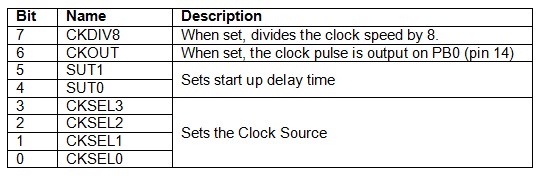
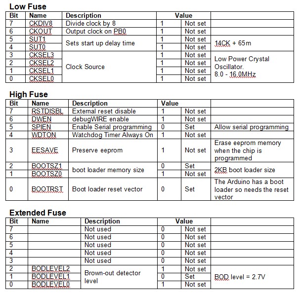
Low Byte Fuses
The low byte fuse deals with the clock source, how fast the chip will run, and how long it waits at startup.
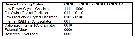
The ATmega chips can be run at different speeds or frequencies and the frequency is determined by the clock source that is used. The clock source is set by using the CKSEL fuse bits.
CKSEL (Clock Sources / Clock Selection)
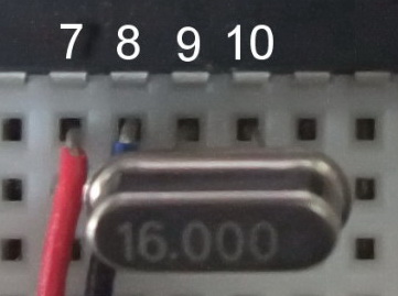
The clock signal can come from an internal oscillator, an external crystal/resonator, or an external signal. Arduinos normally use an external 16MHz crystal.
Here is a 16 MHz crystal used on a bread board Arduino connected to XTAL1 and XTAL2. The ATmega chip has to be told to use the external crystal and this is done by setting the CKSEL bits. A common mistake is to have the crystal correctly connected in the circuit but forget to tell the chip to use it.
The different options for CKSEL are:
Arduinos normally use a low power crystal oscillator.
The ATmega has 2 built in oscillators, a 128kHz RC oscillator and a calibrated RC oscillator.
The external clock option allows the chip to use an external square wave clock signal. This is used when you have a circuit with its own clock that you want to sync the ATmega with or if you want to use a separate clock chip. The external clock signal needs to be connected to the CLOCK-IN pin
Crystal Oscillator Options
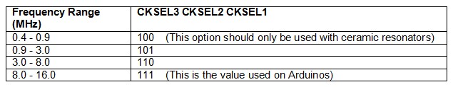
CKSEL3=1 CKSEL2=1 CKSEL1=1 CKSEL0=1 selects a crystal any where from 8MHz to 16MHz and is the normal setting for Arduinos.
If you want to use a slower crystal, for example 6MHz, then you would use CKSEL3=1 CKSEL2=1 CKSEL1=0 CKSEL0=1 (the 3.0 to 8.0 range).
To use the internal RC oscillator at 8MHz, the settings are CKSEL3=0 CKSEL2=0 CKSEL1=1 CKSEL0=0
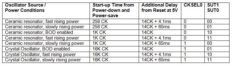
SUT1/SUT0 (Start Up Time)
Crystals and oscillators require sufficient voltage to operate correctly. When you start the ATmega chip it can take a brief period of time for the voltage to get to its maximum value. While the voltage is rising the clock source may not be working at the correct speed or frequency. To allow the clock to stabilise a startup delay can be set.
CKSEL0 is used together with SUT1 and SUT0 to set the start up delay time.
BOD is Brown Out Detection and discussed later.
The Arduino uses the maximum startup delay of 14CK + 65ms (CKSEL0=1, SUT1=1, SUT0=1) which are also the default settings for new ATmega 328/328P chips.
CHDIV8 (Clock Divide)
ATmega 328/328P chips have a built in RC oscillator which has a 8.0MHz frequency. New chips are shipped with this set as the clock source and the CKDIV8 fuse active, resulting in a 1.0MHz system clock. The startup time is set to maximum and time-out period enabled. (CKSEL = “0010”, SUT = “10”, CKDIV8 = “0”). This setting is used so that all users can make their desired clock source setting using any available programming interface.
CKDIV8 should be used if the selected clock source has a higher frequency than the maximum frequency of the ATmega chip.
The ATmega chips can be used at very low voltages, however, the lower the voltage the slower they need to work at. The CHDIV8 can be used to set a slow clock speed to match a low voltage.
CKOUT (Clock Out)
The clock signal can be routed to PB0. This is useful if you need the clock signal to drive other circuits. This works for all clock sources and the default setting for new chips is CKOUT=1 (not set).
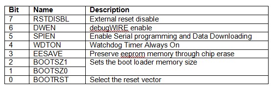
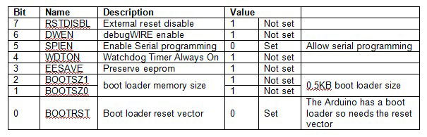
High Byte Fuses
The high byte fuse has several different settings. The ones of normal interest (to me as a hobbyist at least) are the watchdog timer, preserving or erasing eeprom and the boot loader attribute settings.
RSTDISBL (External reset disable)
PC6 is a reset pin, hold it low (to ground) and the chip will reset. This is how the switch on the Arduino works. When you press the reset button it connects PC6 to ground and resets the chip.
PC6 can also be used as a regular IO pin but this means disabling the reset function which in turns means the chip can no longer be inline programmed (in line programming requires a reset). This is one of the options it is better not to change.
I imagine RSTDISBL is implemented for security reasons to stop the chip being reprogrammed or the firmware being downloaded.
When RSTDISBL is programmed the start up time (SUT1 SUT0) is increased to 14CK + 4.1ms to ensure the programming mode can be entered.
By default, the setting is RSTDISBL=1 (not set).
DWEN (debugWIRE enable)
ATmega chips have built in debugging tools which are by default turned off. The DWEN fuse is used to turn them on.
DWEN uses the same pin as reset (PC6) and when DWEN is enabled (and the lock bits are not set) the reset pin becomes a communication pin and normal reset no longer works. For example, if you enable DWEN on an Arduino the reset button no longer works.
To use the on-chip debugging you need a compatible programmer such as the AVR Dragon. Since I have never used AVR studio and do not have a suitable programmer I have never used and do not know how to use debugging. If you would like to know more then there is a good article at http://www.hilltop-cottage.info/blogs/adam/debugging-arduino-using-debugwire-atmel-studio-and-an-avr-dragon/ to get you started.
This is one of the fuses you should take care with. If you enable DWEN and also enable the lock bits you can no longer program the chip in the normal way.
If you are just starting then leave DWEN to not set. After all, reset is very useful.
SPIEN (Enable Serial programming and Data Downloading)
ATmega chips can be programmed using serial programming. Serial programming is used for on board programming using a serial protocol via an ISP (inline serial programmer) or UART (universal asynchronous receiver/transmitter).
The normal method of programming the ATmega chips is via the SPI interface using the SCK (clock), MOSI (input) and MISO (output) pins. If you disable serial programming then you can no longer use the SPI to program the chip. You can also disable serial programming using the lock bits.
For normal use and development leave SPIEN enabled, however, if you have a device that is final and no further programming is required then you can use this option to stop people accessing the chip through serial communication.
The default setting is SPIEN enabled, SPIEN=0.
The RSTDISBL, SPIEN and DWEN fuses have the potential to brick the ATmega chip, or at least make the chip very very difficult to use again. For general use, and especially if you are just starting out with programming stand-alone chips, you should not change these fuse settings. You should also double check that you are not changing them when you re-write the other fuse settings.
WDTON (Watchdog Timer Always On)
The watchdog is basically a timer that will cause the chip to reset if it does not receive an OK signal at specific times.
This can be useful when you have unstable code or have a system that must not be allowed to permanently lock up.
When the watchdog timer is enabled, should a sketch crash or freeze then the timer will time out and reset the chip causing a restart similar to pressing the reset button an a running Arduino.
The Watchdog Timer can be activated in software so the fuse settings doesn’t really need to be used. By default, the watchdog timer is off, WDTON=1.
There is a nice mini guide on the Watchdog timer by za_nic on the Arduino forum at ttp://forum.arduino.cc/index.php/topic,63651.0.html
Paul Martinsen has a guide on how to use the watchdog timer to detect lockups at http://www.megunolink.com/how-to-detect-lockups-using-the-arduino-watchdog/
EESAVE (Preserve EEPROM memory)
When the ATmega chip is programmed the memory is erased just before the new code is uploaded. Under normal circumstances the eeprom memory is erased as well as the program memory. The EESAVE fuse can be used to tell the chip not to erase the eeprom. This is useful when you want to upgrade code but keep user settings that are stored in eeprom.
The default value is EESAVE=1, not set and eeprom memory is erased during the chip erase cycle when programming.
I have got into the habit of setting this fuse; eeprom has a limited life cycle so the less you write to it the better. Erasing the eeprom has no effect on uploading new code and the majority of my projects don’t use the eeprom memory so not erasing it is not a problem. The dropController stores settings and drop times in eeprom and so I set EESAVE to preserve the data when I upload new versions of the code.
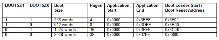
BOOTSZ1 & BOOTSZ0 (Boot loader Size)
The ATmega chips have the ability to use a boot loader, this is a small program that runs when the chip is first started or when it is reset. Boot loaders are normally used to initialize the device and check for external communication. The Arduino uses a boot loader to talk to a connected computer to see if there is a new program to be uploaded. This is the reason the Arduino resets when you upload new code, the reset runs the boot loader, the boot loader checks to see if you have new code.
The boot loader is stored in program memory, the same memory used for the user application and since the boot loader can be different sizes you can tell the ATmega chip how much space to reserve. The regular (older) Arduino boot loader is 2 kilobytes (KB) but the newer Optiboot (used on the UNO) is only 0.5KB (512 bytes). If using Optiboot and setting the boot loader size accordingly you gain an extra 1.5KB for your own program. 1.5KB can be a lot of space, running out of program space is why I started programming stand alone ATmega chips in the first place. The code for the dropController became too large for the regular Arduino so I removed the boot loader.
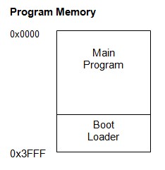
The boot loader is stored at the top of the program memory
If you have a boot loader then BOOTSZ has to be used in conjunction with BOOTRST. BOOTRST tells the ATmega chip the memory address where the boot loader starts. If BOOTRST is not set then the user application can use the whole of the memory regardless of the BOOTSZ settings.
Boot Size Configuration for the 328/328P
Note that the above sizes are in words (a word is 2 bytes) and 256 words is 512 bytes.
The default for new chips is BOOTSZ1=0 BOOTSZ0=0 which means they have 4KB reserved for a boot loader.
BOOTRST Select reset vector
ATmega chips can use a boot loader, this is a small program that runs when the chip is reset. If you have a boot loader then you need to inform the MCU and this is done by using the BOOTRST fuse setting. When the BOOTRST Fuse is set, on reset the device will jump to the Boot Loader address. If not set, the chip will jump to the program start address at 0x0000.
The default value is BOOTRST = 1 (not set).
If BOOTRST is not set (no boot loader) then the BOOTSZ fuses are ignored.
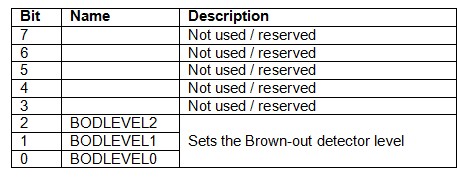
Extended Fuse Bits
The extended fuses are only used to set the brown-out detection level (BOD).
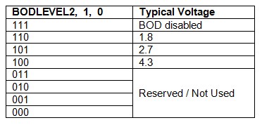
The ATmega chips can become unstable or unreliable when used with insufficient voltage. For example, the 328/328P can run safely at 16MHz if it has at least 4V. Anything below 4V means the chip is likely to misbehave. This would be a problem if the device were being used with sensors to take measurements or relied on accurate timings.
To ensure the chip has sufficient input voltage a minimum voltage level can be set. If the voltage falls below this level then the chip will reset itself. This is called the brown-out detector level. Basically, if the supplied voltage is below the BOD the chip keeps reset low.
The default values for new chips are; BODLEVEL2=1 (not set), BODLEVEL1=1 (not set), BODLEVEL0=1 (not set).
Default Fuse Settings
New ATmega 328P Chip.
New 328/328P chips generally have the following fuse settings:
If you load the Optiboot boot loader then the high byte fuse should be set as 0xDE (B11011110). The only difference is the space allocated to the boot loader.
Lock bits can be used to restrict read/write access to the program memory. The boot section and the application section have their own lock bits and access for each area can be controlled separately.
You can brick the ATmega chip if you enable the lock bits and you should not change them.
I will try to cover lock bits in more detail in a later post.
Actually Programming The Fuses
To program stand-alone ATmega chips I used an Arduino Nano as programmer, see Arduino Nano as an ISP Programmer and found the easiest way to set the fuses was to burn a boot loader (the fuses are set as part of the process). The boot loader can then be written over later when you upload a sketch. By editing the boards.txt file in the Arduino installation folder you can use any values you desire for the fuses.
Here is the entry I added to boards.txt for use with bread board Arduinos. This has the low byte fuse at 0xFF, the hight byte fuse at 0xDF, the extended fuse at 0x05, and uses the Optiboot boot loader. The values for the lock bits were copied from the Arduino Uno entry.
The ATmega 328P data sheet can be down loaded from the Microchip website.
http://eleccelerator.com and http://www.engbedded.com both have a fuse calculator where you select what options you want and the page gives you the fuse settings to use. I prefer not to use the calculators as I think it may be easy to make mistakes but this is my personal opinion only.
NIck Gammon also has a useful sketch that detects ATmega chip types. The sketch can be found at http://www.gammon.com.au/forum/?id=11633. The sketch displays the fuse settings, the lock bits and gives information about the boot loader if one is present. I found this sketch very useful when I first started programming chips directly.